
Setting up a DC microgrid in the lab.


Figure 1: Lab setup of DC microgrid

1. Design of boost converters
DC/DC converters play a major part in renewable microgrids. A general circuit of a boost converter is as shown in figure below. The boost converter consists of a high-frequency power switch that charges and discharges the inductor L and capacitor C through two power electronics switches: a controllable switch Q and a diode D. In this model, the diode on-time resistance, the equivalent series resistance of the capacitor, and switch on-time resistance are ignored. The output voltage of the converter is controlled by controlling the duty cycle of high-frequency input pulses; the higher the frequency of the PWM pulses lowers will be the size of the inductor required. The maximum and minimum duty cycle that is required by a boost converter is given by Equations 1 The power electronic switch quickly charges the inductor to high voltages, and then the inductor will in turn charge the capacitor. The inductor can charge the capacitor to the required voltage level within the ripple voltage limit, as long as the load connected to the output draws the current in such a way the required output voltage level output power drawn is lesser than the input power supplied. Theoretically, input power supplied should be equal to output power drawn, but due to switching and magnetic losses output power is always lesser than the input power.

Figure 2: Boost converter circuit
 
(1)

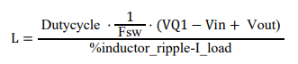
The minimum inductor size required to achieve the required output voltage Vout for an input voltage of Vin is given by Equation 2, and the inductor ripple current ∆Il is given by Equation 3.

(2,3)

In Equation 3, ∆Il is the inductor ripple current and f is the switching frequency of the converter. The minimum size of the output capacitor required to achieve the ripple voltage of ∆Vout is given by Equation 4.

(4)

A boost converter has a non-linear relation between the duty cycle and output voltage due to the non-linear characteristics of the inductor. When an inductor changes, the voltage drops across it decreased exponentially and current through it increases exponentially. The inductor current and voltage have an exponential relation with charging time. The exponential charging characteristics of a boost converter can be seen from Equations 5 and 6.

(5,6,7)

It can be seen from Equations 5 and 6 that the charging time of the inductor is exponentially related to the inductor voltage and inductor current. The output voltage of a boost converter is directly proportional to the voltage dropped across the inductor. For a fixed operating frequency, the duty cycle and output voltage are also going to be related exponentially. This also creates non-linearity between the output voltage and PWM duty cycle in a boost converter.

2. Design of bidirectional buck-boost converters

 
Figure 3: Bidirectional buck boost converter

A bidirectional buck-boost converter is a DC/DC converter that allows the power to flow in both directions. The converter acts as boost converter when the operated no forward mode and the converter will act on buck mode when operated on reverse power flow mode. As it can be seen from figure 3 that the bidirectional boost converter consists of two MOSFETs. When operating on boost mode Q2 is supplied with the PWM and Q1 is only turned on when Q2 is turned off. When Q2 is turned on inductor l1 charges. When Q2 turns off Q1 is turned on and charged inductor discharges through Q1 to the capacitor C2. This process keeps on repeating while the converter is operating on boost, forward power flow mode. When the converter is operated on buck backward power flow mode Q1 acts as a high-speed switch to control the power and Q2 acts as freewheeling MOSFET when Q1 is turned off. Q1 and Q2 are supplied with PWM signals inverted to each other.

When operating on boost mode, the inductor size required for the given converter to generate the required output voltage for the given input voltage is given by equation 8. Similarly, the inductor ripple current is given by equation 8. The minimum capacitor size required on output is given by equation 9. When the converter is operated on buck mode inductor size required is given by equation 13. The inductor for the bidirectional buck-boost converter was selected using equation (7) and equation (8). The inductor satisfies the minimum requirement criteria of both equation (2) and equation (8).

(8)

Similarly, equation 9 shows how a capacitor should be chosen for the input of the converter. The minimum value of the input capacitor should be greater than the value given by equation 9 where Iin is minimum

(9)

3. Hardware setup
Power electronics converters are used in a renewable energy-based microgrid for voltage and frequency control. In a micro-hydro generator where generation is constant, Electronic Load Controllers (ELCs) are used to regulate the voltage and frequency of the generated power. In a wind plant, the generation voltage and frequency vary depending upon the wind speed so, DC-DC or DC-AC, or AC-DC converters are used to regulate the output voltage and frequency depending upon need. In this thesis, a laboratory setup of a DC microgrid is developed where all the generators are considered to generate DC power. In the developed setup two generators along with one storage system are used. In this system, two panels of power 100 watts and 50 watts are used. The generation voltage of each panel was 18 V rated with an open-circuit voltage of 21 V. As the storage a 150 AH, 12 Volts battery was used. Output voltage ripple limit is kept at 0.1 V. Two IRF540 logic-level MOSFETs are used in parallel for switching. The specifications of developed power converters can be seen in Table below.


4. Converters control

Converter 1 and converter 2 are boost converters and converter 3 is a buck-boost converter. Converter 1 and 2 operate in current regulation mode and converter 3 operate in voltage regulation mode. PI controller is used for current and voltage regulation. Logic level MOSFET were used in this setup. To drive the MOSFETs on the converters IR2110 MOSFET driver was used. PI-based feedback controller for boost converter is as shown in Figure 4 and Figure 5. The control parameters are given in table 6 for the converters used in this project. The PWM resolution used in the project was of 12 bits. Similarly, the resolution of the ADCs used in the feedback systems was also 12 bits. The sampling frequency of ADCs were maintained around 1khz for all converters and gate driving frequency was kept at 31khz for all converters. 

Figure 4: PI voltage regulation controller for Buck-boost converter

Figure 5: PI current regulation controller for boost converter

6. Coordination strategy

In renewable energy-based microgrids, there is constant fluctuation in power generation. Because of which the supply capacity of the generator continuously varies. So, there is a need for a central control system that coordinates the power flow between distributed generators. In the developed system storage system acts as a grid forming generator and the rest act as grid supporting generators. The storage system is connected to a buck-boost converter which connects to the bus. Solar generators are connected to the grid with the help of boost converters. These converters normally work in MPPT mode and push the maximum possible current to the bus and also help reduce strain on the grid forming converter. In this way storage system contributes the least possible power while maintaining bus voltage. If the generation is more than demand then the grid voltage will rise above the required level. To bring down the grid voltage back to the required level, the grid forming converter will operate on buck mode and draw a controlled amount of power from the grid to maintain constant bus voltage. The power drawn from the grid will either be used to charge the battery or directed to dump load. Buck-boost converter will help maintain constant bus voltage by drawing power from the bus, however, this mode of operation will put unnecessary strain on the Boost converters on the generator's side. If the power is being dumped to dump load then the SCADA system will be notified about this condition and SCADA will instruct one of the generators to change their mode of operation to controlled current source mode and reduce the power contribution by the same amount which is being drawn by dump load, which will reduce strain on the MOSFETs’ of the converter. This operation will be reversed if there is a power deficiency in the grid. In this system grid forming and current regulation mode-based converters will use PI controller and MPPT converters use Petrov and observe algorithm. Following is the grid coordination strategy proposed in this research. 


In case of any load or generation change event grid forming converter is responsible for maintaining grid voltage. Normally all generators run in MPPT Mode and storage systems on grid forming mode. In this mode of operation two conditions are possible, either the generation is higher or lower than demand. If the generation is higher than demand and the battery is not fully charged excess generation is used to charge the battery, but if the battery is already fully charged the excess power goes to dump load. In this condition, both MPPT converter and Grid forming converters are bearing unnecessary strain, so to reduce strain on the converters SCADA calculates excess power being generated and commands the MPPT converter to act as current source converter and reduce power by the required amount, reducing strain on both Grid supporting and forming converters. After this, if generation is lesser than the demand while grid forming converter is contributing more than 10% of the demand then generation side converters will again go to MPPT mode. In the proposed system, SCADA has a communication time delay of up to 5 seconds. So transient stability of the grid is maintained by grid forming converter due to communication delay in SCADA. However, converters in doing so bear unnecessary strain on themselves. So, SCADA mitigates unnecessary strain in the converters by coordinating the power contribution of the converters in the grid because of which converters run optimally in a steady-state condition. 

5. Hardware implementation

Generation monitoring and control is one of the main functions of the SCADA system. On the generation side, two solar generators of 150 watts and 50 watts are used. Each of the generators is connected to boost converters. The boost converters convert the generation voltage to a steady bus voltage of 48 volts. The power rating of each converter is 150 watts. Similarly, battery storage is also connected to the bus with a buck-boost converter. The power contribution of these systems to the grid is monitored and controlled by the SCADA system. Here boost converter connected to the battery works as a grid forming converter. The main function of this converter is to maintain a steady grid voltage at 48 volts. If the battery system is in discharging state all other converters will act as current source converters and try to inject as much current to the grid, while storage is in charge of maintaining grid voltage. If the generators are generating and injecting enough power into the grid to sustain the grid by themselves then one of the generators will be given the task to act as a grid forming converter after that battery will go to charging mode and act as a load. Similarly, if the second grid forming controller goes to zero power contribution condition, then the last converter will go to voltage regulation mode and maintain the grid. In this way, one of the converters will work as a voltage source and the rest will act as a current source converter. to perform this experimental setup was developed as shown in Figure 51. Figure 52 shows the responce of the system during load fluctuations.

Figure 6: Lab setup
Figure 7:Grid response during load increment event

In Figure 52 red line shows the voltage level and the blue line shows the current in the grid. In this graph channel 1 represent the voltage levels at 5 volts per division and channel 2 shows the current in 1 volt per division. The current data shown is the voltage drop across the 1-ohm shunt resistor. So current per division is 1 A. In this experiment sampling frequency was kept at 1kHz and PWM frequency at 31 kHz. It can be seen that the system responds and adjusts the grid voltage within 50 ms of the fluctuation. 

6. Control strategies

To connect the multiple generators to the grid there is a need for a control system that tells how much power to draw from each generator, which generator should act in grid forming, and the grid following configuration. The stability of the grid in the proposed system will be maintained by the grid forming converter and power coordination in the grid will be done by the SCADA system. when load or generation changes occur in the grid, a grid-forming converter will draw or push the power from or to the grid depending upon the need. If a grid forming converter is pushing power to the grid, then SCADA will check if the power drawn from the generators can be increased. If yes then the SCADA will instruct the generator to increase power contribution which will cause the reduction in power contribution of the grid forming converter (Storage system) as shown in Figure 56

Figure 8: Grid response during load increment event
Figure 9: Grid Response during load decrement event

Similarly, if there is a sudden decrease in load in the system the grid forming converter will draw power from the grid and direct it to dump load. In this condition, the three is excess power in the grid which is causing unnecessary strain on both grid-forming and generation side converter. in this case, SCADA will instruct generation side converters to reduce power contribution by the necessary amount. The response generation side and in this case is as shown in Figure 57.

Popular posts from this blog

CHANGING THE ARDUINO(ATMEGA328) PWM FREQUENCY

CHANGING ARDUINO PWM FREQUENCY In some projects like boost and buck converters we may need to change the default frequency of Arduino PWM pins according to our need in order to control the charging time of inductor. in Arduino UNO pins D5 and D6 have PWM frequency of 62500 HZ , pins D3, D11, D9 and D10 has the default PWM frequency of 31250 HZ . To change the PWM frequency  following code can be written in setup function to set PWM frequency Divide the base frequency of pins by the factor you want to decrease the frequency for each pin  some examples are shown below The divisors available on pins 5, 6, 9 and 10 are: 1, 8, 64, 256, and 1024. The divisors available on pins 3 and 11 are: 1, 8, 32, 64, 128, 256, and 1024. for D3 and D11 TCCR2B = TCCR2B & B11111000 | B00000001; // for PWM frequency of 31372.55 Hz TCCR2B = TCCR2B & B11111000 | B00000010; // for PWM frequency of 3921.16 Hz TCCR2B = TCCR2B & B11111000 | B00000011; // fo

NRF24 based remote with Arduino Nano

MAKING A DRONE REMOTE  to make the drone remote you will need following components:-  nrf24 rf module(two) joystick module(two) arduino nano (two) capacitors (one) now connect the components in following way :- connection of nrf24 for both transmitter and receiver are same. there are some additional connections to be made in transmitter to read data from joystick so and connnect the joystick pins in following way  Right joystick y axis pin = A0;  Right joystick x axis pin  = A7; Right joystick switch pin = A6; left joystick y axis pin = A1;  left joystick x axis pin  = A5;   left joystick switch pin = A2; now after connecting the above circuit upload the following codes given for transmitter and receiver and you will get the data as shown below in receiver side. now transmitter code is as follows #include <SPI.h>  #include "RF24.h" const int Ry = A0; const int Rx = A7; const int Rs = A6; const int Ly

Using PWM with ESP32 boards

  Unlike Arduino boards like UNO, MEGA and many others, ESP32 board does not support analogWrite() command while programming with Arduino IDE. This is because in the Arduino IDE board library for ESP32 does not contain predefined analogWrite( ) function. This is because ESP32 offers many more features with its Digital to Analogue converters, which cannot be fully utilized by analogWrite() function. ESP 32 board can output PWM signals with any frequency the programmer wants upto 40MHZ. but in other arduino boards like arduino uno only selective frequencies are available. ESP 32 also offers DAC resolution upto 16 bits. In this board the relation between ADC resolution and PWM frequency is inverse. The maximum PWM frequency with the currently used ledc duty resolution of 10 bits in PWM module is 78.125 KHz . The duty resolution can be lowered down to 1 bit in which case the maximum frequency is 40  MHz , but only the duty of 50% is available. Available DAC pins in ESP32 can be seen from

ESP8266n based home automation project

   IOT HOME AUTOMATION USING NODE MCU                                                                     In this post you will see how to make a system that lets you control your appliances using a node mcu board . Node mcu board is a development board consisting of a esp8266 wifi module along with programming circuits. you  will need following parts for this project :- 1.NODE MCU board 2.relay module or some relays and transistors 3.matrix board 4.screw connectors or headers 5.5v power supply 6.USB cable now follow the instructions below 1.connect your node mcu to computer and open arduino IDE 2.Now go to preferances and add this url in arduino board manager url       http://arduino.esp8266.com/stable/package_esp8266com_index.json 3.now go to tools/boards/manage boards/ and search and add node mcu board from there 4.now selecet node mcu 1.0 12E board and upload following code to the mcu board. // Load Wi-Fi library #include <ESP8266WiFi.h> //

Voice Based Remote Device Control Using Google Assistant

This post shows that how can we use simple wifi module can be used as internet based home automation device using google assistant and adafruit io. for this project you will need following components and modules:- 1. NODE MCU board                                                             2. Realy board 3. Phone charger now power the node mcu and relay module using the charger and connect the node mcu pins to the relay board  and the hardware is ready now creat the adafruit io account and sign in and creat the feeds and dashboards like below now go to https://ifttt.com/ and creat account and follow following steps  creat a new applet now follow the process in the website to connect the applet to your adafruit io feeds and upload the following code by changing ssid, password, aio key, and user name and you you can control your node mcu pins via google assistant #include <ESP8266WiFi.h> #include "Adafrui

Parallel operation of boost converters in priority-based power sharing mode

Priority based power sharing in parallel connected boost converters is one of the simplest power sharing scheme to run the boost converters in parallel operation. in this simulation it is considered that the boost converters are physically not far from each other, and the controllers of the converters can communicate with other. One of the converters will run on higher priority which means that that converter will supply as much power as it can to the bus, and another will only supply additional power required to maintain bus stability i.e: maintain the bus voltage. Following figure shows the hardware setup of the experiment. Figure: Boost converter parallel operation experimental setup this configuration of the converter is applicable in the conditions where we need to draw as much power from a source as possible and draw only additional power required to maintain bus voltage from the secondary source. An example application case would be when there is a solar and battery-based hom

Closed loop Control of DC to DC boost converter

DC-DC boost converter boosts the DC input voltage to higher DC voltages  according to the duty cycle of  PWM  applied to the mosfet used to charge the inductor.While the mosfet state is on the inductor gets charged, than when the mosfet turns off the voltage stored in inductor and input voltage gets added and appears in the output. But if only these components are used output Voltage will be pulsating and have a frequency similar to that of mosfet switching. So we need to put a capacitor in output in order to oscillating output to smoother output. Still the stored voltage in capacitor will backflow through the mosfet when it is on, So we need to place a diode in between mosfet and capacitor in order to prevent backflow of stored charge in capacitor.After these circuit requirements are completed the boost converter will be boost low voltage DC input to higher DC voltages.The circuit should look like as shown below:- Boost Converter Circuit Output Voltage calculation The

Demand Side Management in a solar microgrid

SCADA in hybrid energy system management and control for isolated DC micro-grid . Our system addresses the problem of connecting different Energy sourced together effectively, monitoring and controlling of the Hybrid energy system formed by different renewable energy sources. Article in the link can be followed for more information. https://www.sciencedirect.com/science/article/pii/S2352484720314554 For our project we developed a small version of DC micro grid taking power from different power sources (Like solar and wind) and combining these sources together   with the help of voltage stabilizing buck-boost converters. After we boot the voltages from different sources to our distribution voltage. We distribute the power for different loads like Households, Hospitals, Schools through dedicated feeders. Now with the help of SCADA  and Sensors we can monitor various system parameters like Generation voltage of different sources, Bus voltage, power consump

Line Follower Robot With Combinational Logic

To make line follower robot using logic circuits only and not using microcontroller we need to make two parts of the circuit .they are:- 1.control logic circuit that turns the robot left when left sensor sences the line and turns right when right sensor senses the line . 2. control circuit to bring the robot back to the line if it goes out of line by recording the data that which sensor senced the line most recently and use that data to turn the robot.   Working video of the project here is the circuit of the system that you need to built followed by description condition 1 condition 2 condition 3 condition 4 condition 5 In above circuits you can see that the robot can come back to the line if it got out of the line using the data stored in the latch the main special  feature of this circuit is that it has one bit memory system that is a latch which helps the robot to come back to the path if it gets lost if you have any question ab