
Project gallery

Some of the photos of my projects that managed to survive long enough on my gallery.


fig : RLDA data acquisition project (2023 February)


fig : DAQ preparation for RLDA (2023 February)

fig : DAQ controller board (2023 February)

fig : DAQ system testing on bump rig (2022 November)


fig: 8 channel strain gauge DAQ system with 10 uV precision
 and 1000 HZ sampling frequency (2022 November)

fig : 8 channel strain gauge DAQ board Ki-CAD PCB (2022 October)

fig: PCB wire tresses (2022 October)
fig : Four channel 24 bit ADC board interfaced
 with teensy4.1 for high speed data acquisition


fig : four channel instrumentational amplifier (2023 January)

fig : Ki-CAD PCB design four channel instrumentation amplifier (2023 October)


fig : Instrumented bike chassis (2022 October)
fig : Half bridge strain gauge application on steel rod (2022 October)

fig : STM 32 pneumatic rig control board (2022 September)

fig : Strain gauge data verification setup (2022 September)

fig : Instrumentation amplifier ADA4254 test board (2022 August)

fig : Ki-CAD design of instrumentation amplifier (2022 June)
fig : instrumentation amplifier test board (LTC6915) (2022 June)


fig : KICAD design of instrumentation amplifier  (LTC6915) (2022 June)

MS by research Graduation


fig : hardware for microgrid setup (2022 April)

fig : load monitoring window
Software developed in Microsoft visual studio ( 2022 march)

fig : microgrid monitoring home screen
Software developed in Microsoft visual studio ( 2022 march)

fig : generation monitoring window
Software developed in Microsoft visual studio ( 2022 march)

fig : Communication setup window
Software developed in Microsoft visual studio ( 2022 march)
fig : Project information window
Software developed in Microsoft visual studio ( 2022 march)

fig : DC microgrid setup (2022 February)

fig : DC microgrid setup (2022 February)

fig : DC microgrid setup (2022 February)

fig : DC microgrid setup (2022  January)

fig : DC-DC boost converter model predictive control experimental setup (2021 December)

fig : boost converter operating regions vs voltage output at fixed load (2021 December)

fig : DC-DC boost converter test setup to find the converter characteristic
at different operating regions (2021 December)

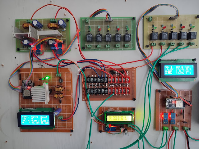
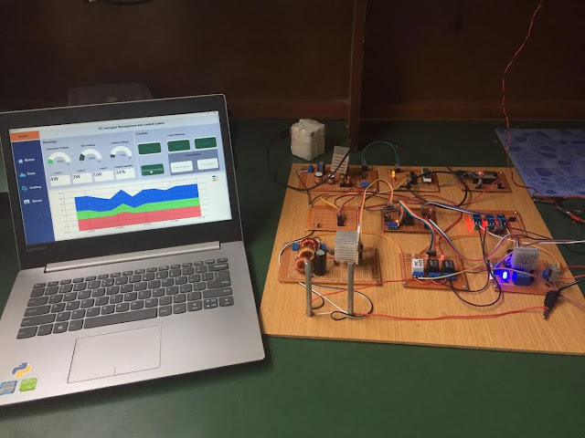
fig : Initial microgrid setup (2021 November)

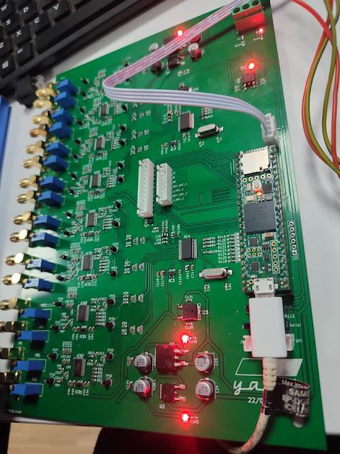
 fig : Lora based energy meter (2021 October)

fig : Energy meter firmware development and testing (2021 September)

fig : energy meter developed in Kathmandu university 
microgrid lab (2021 September)

fig :Programmable relay board developed at Kathmandu university
 microgrid lab (2021 September)

fig : Energy meter PCB board (2021 September)

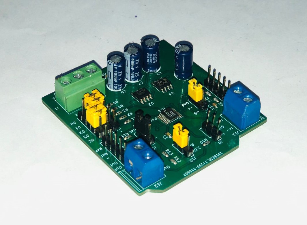
fig : MPPT charge controller PCB board (2021 September)

fig :Programmable relay board (2021 September)

fig : MPPT charge controller test (2021 September)

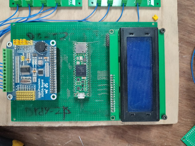
fig : Lora based Energy meter network test site at Gorkha district (2021 August)

fig : Lora mesh network test site at Kathmandu University premises (2021 July)


fig : LoRa Mesh network test node

fig : LoRa mesh simulation on NS2 software (2021 July)

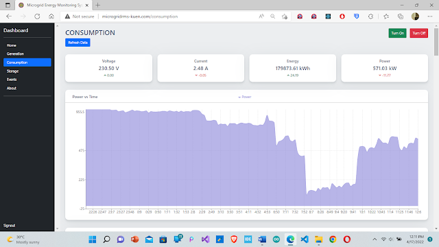
fig : energy monitoring website developed for Marangburu microgrid 
located at Biratnagar Nepal (2021 july)

fig : LoRa mesh software development (2021 June)

fig : DC-  DC bidirectional Buck-Boost converter testing (2021 June)

fig : LoRa energy meter preliminary hardware test (2021 June)

fig : SPWM inverter hardware setup (2021 May) 

fig : Wifi based energy meter test (2021 May)


fig : Experiment to measure phase angle between current and voltage
I was easily able to detect phase angle and was trying to find a 
way to determine whether the measured angle is lead or lag via code. (2021 March)

fig : SPWM pulses generated for inverter (2021 March)

fig : MPPT solar charge controller experimental setup


fig : A4 size CNC plotter  (2021 February)

fig : CNC plotter result (2021 February)

fig : CNC plotter result (2021 February)

fig : CNC plotter result (2021 February)

fig : CNC plotter result (2021 February)


fig : DVD driver CNC plotter 2021 (January)

fig : DVD driver CNC plotter (2021 January)

fig : work table (2021 January)

fig  :Motor control lab KU DOEEE (2020 November)

fig: Priority based load sharing simulation of DC-DC converters 
(2021 October)

fig : project framework development MS by research (2020 march )

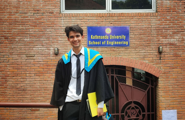
Bachelors in Electrical and Electronics Engineering Graduation


fig : Internship SCADA design for Upper Mai Hydropower ( 2019 October)

fig : Internship HMI design (2019 October)

fig : Internship HMI design (2019 October)

fig : Bottle filling plant PLC setup (Internship 2019 October)

fig : Internship PLC programming setup (2019 October)

fig : Microcontroller training program (2019 August)

fig : fourth year project setup (2019 August)

fig : fourth year project setup (2019 August)

fig : Rural Nepal household load profile survey (2019 4th year) 

fig : Light intensity controller software ( 2019 4th year)

fig : Relay switching board ( 2019 4th year)

fig : 8 channel nrf24 based wireless receiver ( 2019 4th year)

fig :Nrf24 based remote controller ( 2019 4th year)

fig : esp32 SD card data logger ( 2019 4th year)

fig : ATmega328 based boost converter controller
 ( 2019 4th year)


fig : LM35  based seven segment temperature
 measurement circuit ( 2019 4th year)

fig : IOT based contactor controller 
(2019 4th year)


fig : Energy meter (2019 4th year)

fig : microcontroller training program (2018 3rd year)

fig : Patient monitoring system for hospitals 
(3rd year project 2018)

fig : Patient monitoring system for hospitals 
(3rd year project 2018)

fig : Optical pulse sensor serial plot 
(3rd year 2018)


fig : IOT based waste management system 
(3rd year 2018) 
(IT meet  Hardware hackathon)

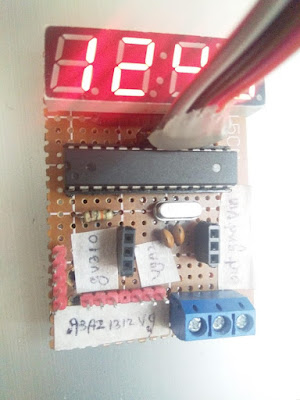
 fig : ATmega328 based clock (3rd year 2018)


fig : Power supply design for electronics projects
(3rd year 2018)

Fig : IOT based home automation board
(3rd year 2018)

fig : Bottle hackathon 2018
(3rd year 2018)

fig : Line following robot sensor array development 
(2nd year 2017)

fig : Line follower combinational logic PCB 
(2nd year 2017)

fig : Line follower robot logic development
(2nd year 2017)


fig : ATmega328 development board PCB
(2nd year 2017)

fig : Motor driver PCB
(2nd year 2017)

fig : IR sensor array PCB
(2nd year 2017)
fig : combination logic based line follower
 robot with 1 bit memory PCB
(2nd year 2017)

fig : project day (2nd year 2017)


fig : 2nd year project 
(combinational logic based line follower with 1 bit memory)
 (2nd year 2017)

fig : Environmental data collection device 
Barometric pressure, temperature , ultrasonic distance measurement
CO2 level measurement
(2nd year 2017)


fig : first year Arduino training ( 1st year 2016)


Popular posts from this blog

CHANGING THE ARDUINO(ATMEGA328) PWM FREQUENCY

CHANGING ARDUINO PWM FREQUENCY In some projects like boost and buck converters we may need to change the default frequency of Arduino PWM pins according to our need in order to control the charging time of inductor. in Arduino UNO pins D5 and D6 have PWM frequency of 62500 HZ , pins D3, D11, D9 and D10 has the default PWM frequency of 31250 HZ . To change the PWM frequency  following code can be written in setup function to set PWM frequency Divide the base frequency of pins by the factor you want to decrease the frequency for each pin  some examples are shown below The divisors available on pins 5, 6, 9 and 10 are: 1, 8, 64, 256, and 1024. The divisors available on pins 3 and 11 are: 1, 8, 32, 64, 128, 256, and 1024. for D3 and D11 TCCR2B = TCCR2B & B11111000 | B00000001; // for PWM frequency of 31372.55 Hz TCCR2B = TCCR2B & B11111000 | B00000010; // for PWM frequency of 3921.16 Hz TCCR2B = TCCR2B & B11111000 | B00000011; // fo

NRF24 based remote with Arduino Nano

MAKING A DRONE REMOTE  to make the drone remote you will need following components:-  nrf24 rf module(two) joystick module(two) arduino nano (two) capacitors (one) now connect the components in following way :- connection of nrf24 for both transmitter and receiver are same. there are some additional connections to be made in transmitter to read data from joystick so and connnect the joystick pins in following way  Right joystick y axis pin = A0;  Right joystick x axis pin  = A7; Right joystick switch pin = A6; left joystick y axis pin = A1;  left joystick x axis pin  = A5;   left joystick switch pin = A2; now after connecting the above circuit upload the following codes given for transmitter and receiver and you will get the data as shown below in receiver side. now transmitter code is as follows #include <SPI.h>  #include "RF24.h" const int Ry = A0; const int Rx = A7; const int Rs = A6; const int Ly

Using PWM with ESP32 boards

  Unlike Arduino boards like UNO, MEGA and many others, ESP32 board does not support analogWrite() command while programming with Arduino IDE. This is because in the Arduino IDE board library for ESP32 does not contain predefined analogWrite( ) function. This is because ESP32 offers many more features with its Digital to Analogue converters, which cannot be fully utilized by analogWrite() function. ESP 32 board can output PWM signals with any frequency the programmer wants upto 40MHZ. but in other arduino boards like arduino uno only selective frequencies are available. ESP 32 also offers DAC resolution upto 16 bits. In this board the relation between ADC resolution and PWM frequency is inverse. The maximum PWM frequency with the currently used ledc duty resolution of 10 bits in PWM module is 78.125 KHz . The duty resolution can be lowered down to 1 bit in which case the maximum frequency is 40  MHz , but only the duty of 50% is available. Available DAC pins in ESP32 can be seen from

ESP8266n based home automation project

   IOT HOME AUTOMATION USING NODE MCU                                                                     In this post you will see how to make a system that lets you control your appliances using a node mcu board . Node mcu board is a development board consisting of a esp8266 wifi module along with programming circuits. you  will need following parts for this project :- 1.NODE MCU board 2.relay module or some relays and transistors 3.matrix board 4.screw connectors or headers 5.5v power supply 6.USB cable now follow the instructions below 1.connect your node mcu to computer and open arduino IDE 2.Now go to preferances and add this url in arduino board manager url       http://arduino.esp8266.com/stable/package_esp8266com_index.json 3.now go to tools/boards/manage boards/ and search and add node mcu board from there 4.now selecet node mcu 1.0 12E board and upload following code to the mcu board. // Load Wi-Fi library #include <ESP8266WiFi.h> //

Voice Based Remote Device Control Using Google Assistant

This post shows that how can we use simple wifi module can be used as internet based home automation device using google assistant and adafruit io. for this project you will need following components and modules:- 1. NODE MCU board                                                             2. Realy board 3. Phone charger now power the node mcu and relay module using the charger and connect the node mcu pins to the relay board  and the hardware is ready now creat the adafruit io account and sign in and creat the feeds and dashboards like below now go to https://ifttt.com/ and creat account and follow following steps  creat a new applet now follow the process in the website to connect the applet to your adafruit io feeds and upload the following code by changing ssid, password, aio key, and user name and you you can control your node mcu pins via google assistant #include <ESP8266WiFi.h> #include "Adafrui

Parallel operation of boost converters in priority-based power sharing mode

Priority based power sharing in parallel connected boost converters is one of the simplest power sharing scheme to run the boost converters in parallel operation. in this simulation it is considered that the boost converters are physically not far from each other, and the controllers of the converters can communicate with other. One of the converters will run on higher priority which means that that converter will supply as much power as it can to the bus, and another will only supply additional power required to maintain bus stability i.e: maintain the bus voltage. Following figure shows the hardware setup of the experiment. Figure: Boost converter parallel operation experimental setup this configuration of the converter is applicable in the conditions where we need to draw as much power from a source as possible and draw only additional power required to maintain bus voltage from the secondary source. An example application case would be when there is a solar and battery-based hom

Setting up a DC microgrid in the lab.

  Figure 1: Lab setup of DC microgrid 1. Design of boost converters DC/DC converters play a major part in renewable microgrids. A general circuit of a boost converter is as shown in figure below. The boost converter consists of a high-frequency power switch that charges and discharges the inductor L and capacitor C through two power electronics switches: a controllable switch Q and a diode D. In this model, the diode on-time resistance, the equivalent series resistance of the capacitor, and switch on-time resistance are ignored. The output voltage of the converter is controlled by controlling the duty cycle of high-frequency input pulses; the higher the frequency of the PWM pulses lowers will be the size of the inductor required. The maximum and minimum duty cycle that is required by a boost converter is given by Equations 1 The power electronic switch quickly charges the inductor to high voltages, and then the inductor will in turn charge the capacitor. The inductor can charge the cap

Closed loop Control of DC to DC boost converter

DC-DC boost converter boosts the DC input voltage to higher DC voltages  according to the duty cycle of  PWM  applied to the mosfet used to charge the inductor.While the mosfet state is on the inductor gets charged, than when the mosfet turns off the voltage stored in inductor and input voltage gets added and appears in the output. But if only these components are used output Voltage will be pulsating and have a frequency similar to that of mosfet switching. So we need to put a capacitor in output in order to oscillating output to smoother output. Still the stored voltage in capacitor will backflow through the mosfet when it is on, So we need to place a diode in between mosfet and capacitor in order to prevent backflow of stored charge in capacitor.After these circuit requirements are completed the boost converter will be boost low voltage DC input to higher DC voltages.The circuit should look like as shown below:- Boost Converter Circuit Output Voltage calculation The

Demand Side Management in a solar microgrid

SCADA in hybrid energy system management and control for isolated DC micro-grid . Our system addresses the problem of connecting different Energy sourced together effectively, monitoring and controlling of the Hybrid energy system formed by different renewable energy sources. Article in the link can be followed for more information. https://www.sciencedirect.com/science/article/pii/S2352484720314554 For our project we developed a small version of DC micro grid taking power from different power sources (Like solar and wind) and combining these sources together   with the help of voltage stabilizing buck-boost converters. After we boot the voltages from different sources to our distribution voltage. We distribute the power for different loads like Households, Hospitals, Schools through dedicated feeders. Now with the help of SCADA  and Sensors we can monitor various system parameters like Generation voltage of different sources, Bus voltage, power consump

Line Follower Robot With Combinational Logic

To make line follower robot using logic circuits only and not using microcontroller we need to make two parts of the circuit .they are:- 1.control logic circuit that turns the robot left when left sensor sences the line and turns right when right sensor senses the line . 2. control circuit to bring the robot back to the line if it goes out of line by recording the data that which sensor senced the line most recently and use that data to turn the robot.   Working video of the project here is the circuit of the system that you need to built followed by description condition 1 condition 2 condition 3 condition 4 condition 5 In above circuits you can see that the robot can come back to the line if it got out of the line using the data stored in the latch the main special  feature of this circuit is that it has one bit memory system that is a latch which helps the robot to come back to the path if it gets lost if you have any question ab